激光干涉仪半导体应用 SEMICONDUCTOR
IDS3010皮米分辨率激光干涉仪
Real-Time Displacement Sensor for Machine Integration

半导体典型应用:
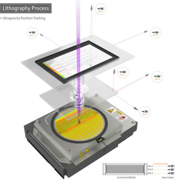
超高精度位置追踪
动态运动控制
平面检测-阵列探测器
支持10MHz带宽高速采样。
支持最高被测物运动速度2m/s。
支持30m以上超长距离。
皮米级分辨率,高精度测量。
支持数十轴测量。
Ultraprecise Position Tracking Application/Challenge:
超精密位置追踪应用
在光刻过程中,纳米级的电路图案从光学掩模板中通过透镜组转到半导体硅片上。光学掩模板图案被投影到硅片上,硅片台子移动,光刻过程不断重复,直到这个硅片覆盖足够的电路图案。解决方案 IDS3010提供真空,高温兼容探头,可以很轻松将探头集成到光刻设备上,保证关键元件装调达到纳米级别精度,数据传输带宽高达10MHz。
在光刻过程中,为了保证高质量光刻,测量结构,光学和硅片平台都的高精度位置追踪和调整是至关重要的。所有原件需要满足洁净间要求,根据现有技术条件,可以将整套测试方案置于真空,超高温环境中。
During the photolithography process circuit patterns of few nanometers in size are transferred from the photomask (reticle) via various lenses onto the semiconductor wafer. After the photomask pattern is projected to one part of the wafer, the wafer stage is moved and the lithography process is repeated until the whole wafer is covered with the respective patterns.
attocube’s Solution:attocube ́s laser interferometer IDS3010 with vacuum and high temperature compatible sensor heads can be easily integrated into lithography machines, ensuring the best alignment among the key components with nanometer accuracy, delivering high speed data with up to 10 MHz bandwidth.The ultraprecise position tracking and alignment of measurement frame, optics and wafer stage is key condition to ensure highest quality throughout the lithography process. All components used in this process need to meet the requirements of clean room conditions and – depending on the technology – be capable to perform under vacuum and high temperature environments.

Dynamic Motion Control
动态运动控制
掩模平台和硅片平台都需要在数米的行程下实现快速高精度运动。任何用于运动控制的测量设备精度和速度都需要比光刻过程中运动设备精度高一个数量级。
IDS31010在5m的测量范围,可以测量运动目标高达2m/s,保证了半导体测量应用中对精度的要求。
Reticle and wafer stages need to perform long stroke movements of up to several meters that are both fast and precise. Any measurement device for motion control has to be an order of magnitude more precise and fast than the process itself.
attocube ́s laser interferometer IDS3010 enables metrology tools to achieve the required precision at nanometer range over long distances up to 5 meters with a target velocity of up to 2 m/s.


Planarity Detection
平面检测
在光刻和测量过程中,硅片需要中极端环境下做高速运动,且受到多个方向的作用力影响。这个会引起硅片的弹性形变和塑性形变,从而影响硅片的平面度。不规则硅片会降低光刻精度,计量结果分析结果也会发生偏离。例如采用磁驱的硅片运动平台在运动过程中,平面的表面在垂直方向产生变形。为了优化硅片平台的操作模式,减少光刻过程中硅片的形变,需要一种纳米级超高精度,无接触硅片形变量测量。
IDS3010可以直接测量硅片,或者反射镜上纳米级的形变量。探头结构较小,可以同时测量硅片上不同位置的形变,获得多维形变信息。这同样可以用于极端环境,如真空或者恶劣环境下。
During the lithography and metrology processes the wafer is exposed to extreme environments, fast motions and multi-dimensional forces. These could cause elastic or plastic deformation of the wafer which influences the wafers planarity. Uneven wafers reduce the accuracy of lithography processes and distract results of metrology analyses.For example the movement of wafer stages working with magnetic levitation deforms in direction perpendicular to the flat surface of the plate. The operating status of the wafer stage motor influences the level of deformation. To optimize the operation mode of wafer stages and therefore reduce the wafer deformation during lithography process, a nano- precise and contactless detection of wafer deformation is required.
attocube ́s laser interferometer IDS3010 is capable of measuring directly on the wafer or on mirrors to capture deformations in nanometer range. The miniaturized design of the sensor heads allows to measure the de- formation at several places on the same wafer to detect more-dimensional deformations. It can be used under extreme environmental conditions such as vacuum or other harsh environments.


